
Flexble PCB Manufacturer
A flexible printed circuit board (PCB) is a type of PCB that is designed to be flexible, rather than rigid like traditional PCBs. These types of boards are made from thin, flexible materials such as polyimide or PET (polyethylene terephthalate), and they are used in a variety of applications where a traditional PCB would not be suitable due to space or design constraints.

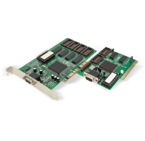
Flexble PCB Manufacturing Solutions
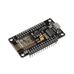
What is Flexible PCB? Flexible PCB, also known as flex prints or flex circuits, is a special type of circuit board that you can bend into the desired shape. They are widely used for high-density and high-temperature applications.Flexible PCBs can be bent, twisted, or folded to fit into a desired shape or space, making them ideal for use in compact devices or in applications where the PCB needs to be conformal to a specific surface. They are also useful in applications where the PCB needs to be flexible in order to withstand mechanical stress or vibration.Some common applications for flexible PCBs include wearable devices, flexible displays, and portable electronic devices. They are also used in automotive, medical, and military applications. Flexible PCBs are typically manufactured using a process called etching, in which a thin layer of copper is applied to the surface of the flexible material and then patterned using photolithography and etching to create the desired circuit traces. The flexible PCB is then coated with a protective layer to prevent corrosion and damage.
We can provide to...
- Turn times as short as 24 hours
- 1 to 100,000 units
- Class II Inspection standard and Class III Inspection available
- 100% on-time guarantee
- DFM support
- Lead free (RoHS) options
- SMT and thru-hole capabilities
- All SMT machine placed
- AOI (Automated Optical Inspection)
- Lead-free RoHS Certification and ITAR compliance screen available
-
Program Design
-
flex Board Capability
-
PCB manufacturing Capabilities
-
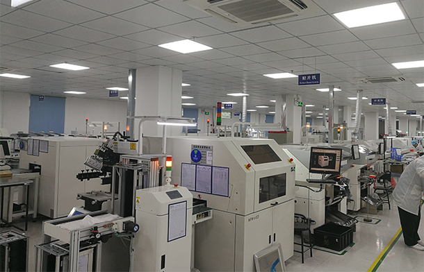
Equipment Exhibition
From component purchasing to function test and package finish , we provide one shop stop services for every types of PCB.
Quick payment
Flexible payment options
On-Demand Manufacturing
No MOQ or MPQ limited. Prototype or mass production order acceptable.
Inspection Of Quality
90% of the technical staff have more than 10 years of industry experience
flex Board Capability
| Layer Count | 1-6L 1-4 L normal |
| Board Thickness | 0.1-0.5mm (1-4L) 0.6-0.8mm (5-6L) |
| The tolerance of 1L board thickness | ±0.03mm |
| The tolerance of 2L board thickness | ±0.03mm |
| The tolerance of multilayer board thickness | ±10% (Normal ±0.1mm) |
| The tolerance of multilayer board thickness | ±10% (Normal ±0.05mm) |
| The tolerance of board thickness | ±10% (Normal ±0.1mm) |
| The tolerance of board thickness | 9inch*23inch(PI≥1mil) 9inch*14inch (normal) |
| Max finished board size | 2mm*4mm(no connection tab);8mm*8mm(with connection tab) |
| Min finished board size | 生益 SF305: PI=0.5mil, 1mil, 2mil; Cu=0.33OZ, 0.5OZ, 1OZ |
| Adhesive flex core | 杜邦AP:PI=1mil,2mil,3mil,4mil;Cu=0.5oz,1oz, 2oz |
| Adhesiveless core | 杜邦AP:PI=1mil,2mil,3mil,4mil;Cu=0.5oz,1oz, 2oz |
| Thermosetting adhesive | 杜邦LF:0110,0210 |
| PI stiffener | 台虹 MHK 系列: PI=3mil, 5mil , 7mil, 9mil |
| 3M tape | 9077,9460 |
| Finished copper thickness 12um / 18um | 3/3mil |
| Finished copper thickness 35um | 4/3.5mil |
| Finished copper thickness 70um | 6/5mil |
| Solder mask bridge min. (copper thickness<=1oz) | 4mil(Green),5mil(White),8.0mil(big copper area) |
| Solder mask opening (single side) | 6mil,8mil(big copper area) |
| Solder mask opening of NPTH (single side) | 3mil(partial2.5mil) |
| Min. coverlay bridge | 8mil |
| Finished copper thickness 12um / 18um | 5/5mil (after compensation) |
| Finished copper thickness 35um | 6.5/5mil (after compensation) |
| Finished copper thickness 70um | 10/8mil (after compensation) |
| Min. Inner layer annual ring width | 4mil(<4L),7mil(4-6L),9mil(7-8L) |
| The min distance between inner layer isolated pad and copper area | 3.5mil 4mil normal |
| Max finished inner layer copper thickness | 3oz 2 oz normal |
| Finished copper thickness, before compensation | 3/3mil |
| Finished copper thickness 35um, before compensation | 3.5/3.5mil |
| Finished copper thickness 70um, before compensation | 5.5/5mil |
| Finished copper thickness 35um, | 3mil(<2mm);4mil(2-4.5mm) |
| Finished copper thickness 35-70um, | 5mil(<2mm);6mil(2-4.5mm) |
| Finished copper thickness >70um, | 7mil(<2mm);10mil(2-4.5mm) |
| Min the distance between NPTH edge to external conductor before compensation | 4oz 2 oz normal |
| Max finished external copper thickness | 8mil 5mil(Gold finger area) |
| The max board thickness for 0.15mm drill bit | 0.8mm |
| Min laser hole diameter | 0.1mm |
| Min finish half PTH via diameter | 0.3mm |
| Min NPTH tolerance | ±2mil(limit+0,-2mil or +2mil,-0) |
| Min space between via hole walls in different net, before compensation | 10mil(after compensation) 12mil (normal)(after compensation) |
| Tolerance of stiffener tape | ±0.1mm (Normal ±0.2mm) |
| Tolerance of Coverlay | ±2mil ((Normal ±4mil) |
| Min distance between coverlay opening and conduct | 3mil ((Normal 4mil) |
PCB manufacturing Capabilities
| Normal Tg FR4(Halogen free) | Shengyi S1150 |
| High Tg FR4(Halogen free) | Shengyi S1165 |
| HDI PCB material | LDPP(IT-180A 1037,1086)、Normal 106,1080 |
| High Tg FR4 | Isola:FR408、FR408HR、IS410、FR406、GETEK、PCL-370HR |
| Ceramic Particle Filled Laminates | Rogers:Rogers4350、Rogers4003;Arlon:25FR、25N; |
| PTFE Laminates | Rogers、Taconic、Arlon、Nelco、TP |
| PTFE PP | Taconic:TP、TPN、HT1.5(1.5mil)、Fastrise |
| Rigid PCB | Back board、HDI、 |
| Blind&buried via type | Laminating≤3 times |
| HDI PCB | 1+n+1、1+1+n+1+1、2+n+2、3+n+3 |
| Lead free | Flash gold、ENIG |
| aspect ratio | 10:01:00 |
| Max finished size | HAL Leaded 22"*39" |
| MIN finished size | HAL Leaded 5"*6" |
| PCB thickness | HAL Leaded0.6-4.0mm; |
| MAX high to gold finger | 1.5inch |
| Min space between gold fingers | 6mil |
| Min block space to gold fingers | 7.5mi |
| Max lamination cycle | 3 times |
| Min laser drill for stacked via | 0.1mm |
| Min stacked via pad size | 0.3mm |
| Max laser drilling size | 0.15mm |
| Blind Via Finished Hole Size | 0.3mm |
| Buried Via Finished Hole Size | 0.3mm |
| Non Conductive Filled Vias | 0.2mm~0.8mm |
| Conductive Filled Vias | 0.2~0.8mm |
| ENIG (Electroless Nickel/Immersion Gold) | AU: 0.05~0.1um Nickel: 3~5um |
| Hard gold | 0.1~1.0um |
| Soft gold | 0.1~1.0um |
| Lead Free HASL | 2~40um |
| Flash gold(electroplated gold) | Au 0.025-0.10um,Nickel 3~5um |
| electroplated Gold finger | Au 0.25-1.0um Nickel 3~5um |
| Selective Gold | Au 0.25-1.0um Nickel 3~5um |
| Tin Nickel | N/A |
| Immersion Silver | 0.2~0.4um |
| Soldermask | min. 8um, max. 30um |
| Min mechanical hole 4mil/6mil/8mi | 0.8mm/1.5mm/2.5mm |
| Finshed mechanical hole size | 0.1~6.0mm |
| MAX aspect ratio for Hole | 12:01:00 |
| Max aspect ratio for mechanical depth- control | 1.3:1 |
| Min. depth of Mechanical depth- control(backdrill) | 0.2mm |
| Min gap between hole wall conductor | 7mil |
| Min space between laser holes and conductor | 5mil |
| Min space bwteen hole walls in different net | 12mil |
| Min space bwteen hole walls in same net | 8mil |
| Min space bwteen NPTH hole walls | 10mil |
| Hole location tolerance | '+/-3mil |
| NPTH tolerance | '+/-0.05mm |
| Pressfit holes tolerance | '+/-0.05mm |
| Countersink depth tolerance | '+/-0.15mm |
| Countersink hole size tolerance | '+/-0.15mm |
| Min Pad size for laser drillings | 0.25mm |
| Min Pad size for mechanical drilling | 0.4mm |
| Min Pad size for mechanical drilling | 0.3mm |
| Min BGA pad size | 0.4mm |
| Pad size tolerance(BGA) | '+/-2mil |
| Min lead pitch | 0.3mm |
| Min BGA ball pitch | 0.3mm |
| Internal Layer | 1/3OZ: N/A |
| Internal Layer | 1/2OZ: 3.5/3.5mil |
| Internal Layer | 1OZ: 3/4mil |
| Internal Layer | 2OZ: 4/5mil |
| External Layer | 1/3OZ: 3/3mil |
| External Layer | 1/2OZ:3.5/3.5mil |
| Width tolerance | ≤10mil:+/-20% |
| Min copper pour to Pour | 7mil |
| Min copper pour to trace | 4mil |
| Min copper pour to microvia | 8mil |
| Min copper pour to buired via | 4mil |
| Min copper pour to SMD Pad | 5mil |
| Min copper pour to PTH Pad | 5mil |
| Soldermask color | Semi Gloss greeen\Gloss Green\Matte Green\Black\Red\Blue\Yellow |
| Solder Mask Min Dam Size | 4mil |
| Solder Mask Min Dam Size in BGA Area | 4mil |
| Solder Mask Registration | '+/-4mil |
| Silkscreen color | White, yellow , black |
| Min width of soldermask bridge | White, yellow , black |
| Min width of soldermask bridge | 4mil |
| Min. Diameter Rout Cutter Available | 0.6mm |
| Routed Part Size Tolerance | '+/-0.15mm |
| V-CUT symmetrical tolerance | '+/-0.1mm |
| MAX V-CUT lines | 80 lines |
| V-CUT angle tolerance | '+/-5 degress |
| V Score, Edge to Copper | H≤1.0mm:0.3mm(20°)、0.33mm(30°)、0.37mm(45°); |
| V Score, Edge to Copper | 1.0<H≤1.6mm:0.36mm(20°)、0.4mm(30°)、0.5mm(45°); |
| V Score, Edge to Copper | 1.6<H≤2.4mm:0.42mm(20°)、0.51mm(30°)、0.64mm(45°); |
| V-CUT angle | 20、30、45 degree |
| Gold finger bevelling | 20、30、45、60 degree |
| Gold finger bevelling tolerance | '+/-5 degree |
| Min space of gold finger chamfering | 6mm |
| Min gap between the side of | 8mil |
| Layer count | 1~28 layer |
| PCB thickness | 0.4~6..0mm |
| PCB thickness tolerance˄Normal | Thickness : ±10%(>1.0mm);±0.1mm(≤1.0mm); |
| PCB thickness tolerance˄Special ˅ | Thickness ±0.1mm(≤2.0mm);±0.15mm(2.1-3.0mm) |
| Min bow&twist | 0.75% |
| Controlled Impedance Tolerance | '+/-10% |
| Testing methods | Flying probe testing, Test fixture |
| Quality standards | IPC II, IPC III |
Testing Procedures
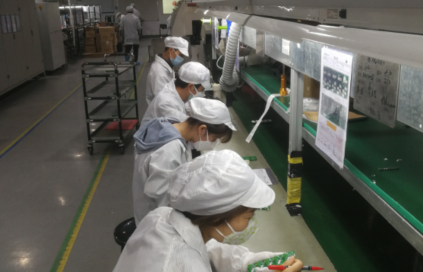
Flexible printed circuit boards (FPCBs) are a type of circuit board that is made from flexible materials, such as polyimide or polyester, and are used in a wide range of electronic applications. The manufacturing capacity of a flexible PCB manufacturer refers to the maximum amount of FPCBs that the manufacturer can produce in a given period of time.
There are several factors that can impact a flexible PCB manufacturer’s manufacturing capacity, including the equipment and technology used, the efficiency of the manufacturing process, and the availability of skilled labor. Some flexible PCB manufacturers may have a higher manufacturing capacity due to their use of advanced equipment and automation, while others may have a lower capacity due to a reliance on manual processes or a smaller workforce.
It is important for flexible PCB manufacturers to carefully manage their manufacturing capacity in order to meet the demand for their products and to maximize efficiency and profitability. This may involve investing in new equipment or technology, training workers, or optimizing the manufacturing process to increase productivity.


Bring you better PCB products
Circuit Board Fabrication and PCB Assembly Turnkey Services
Flexble PCB asked questions
What are flexible PCBs used for?
How are flexible PCBs made?
What are the advantages of using flexible PCBs?
What are the limitations of flexible PCBs?
The received assembled PCB's worked flawlessly. The placement of the parts is excellent. I had a very good contact with Mis wang the WINOW engineer who took care of our project. She asked the right questions to make sure the project was finished correctly. We had a very pleasant communication, fast and to the point.
This board is needed to charge the lipo batteries of my robotic platform (rover). First time order with excellent communications throughout the ordering, manufacturing progress and up to delivery tracking. Very good price especially the first order with a discount credit.
Boards arrived yesterday and got started on assembly. Excellent, solder wetting, clean line
definition, via drill holes exactly in the middle of via lands.
Please pass my thanks back to one and all who made such excellent boards.
Why Choose Us?
Since 2018, WINOW has offered good-quality PCBs with excellent turnaround times and customer satisfaction. We are one of the biggest and most skilled board manufacturers in China.
-
 Prototype orders placed within 24 hours
-
Normal lead time (5-7 Working days for some PCBs prototypes and small batch production)
-
Faster lead time (48 hours for some PCBs prototypes and small batch production)
Quick payment
Flexible payment options
On-Demand Manufacturing
No MOQ or MPQ limited. Prototype or mass production order acceptable.
Inspection Of Quality
90% of the technical staff have more than 10 years of industry experience
Technical Strength
ICT test, veneer test, aging test, ATE test can be adjusted at any time PCB Assembly according to customer requirements