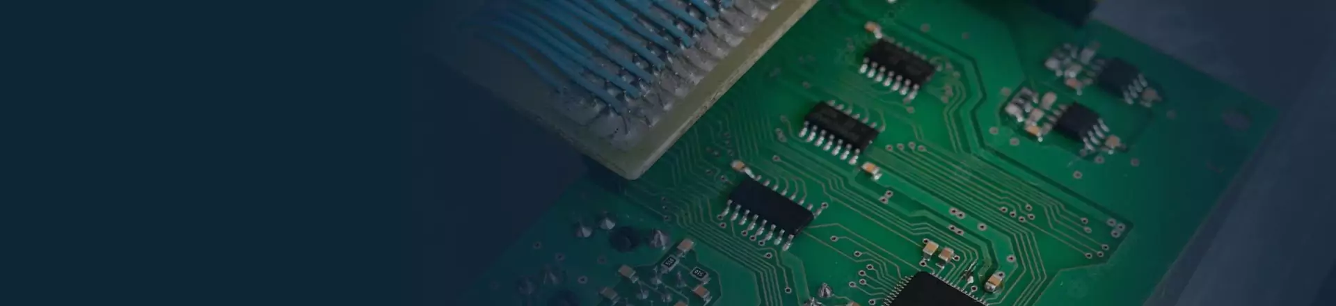
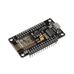
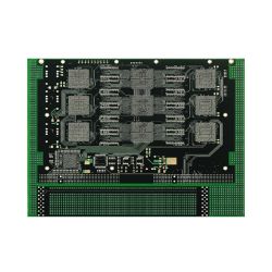
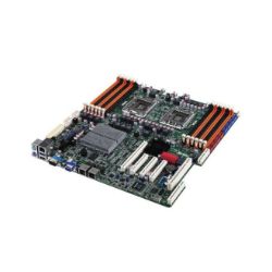
Through Hole PCB Assembly
Through-hole PCB assembly is a manufacturing process in which components are mounted onto a printed circuit board (PCB) by inserting their leads or pins through holes in the PCB and soldering them in place. This method was traditionally used in the production of PCBs and is still in use today, although it has largely been replaced by surface mount technology (SMT) in mass production.

Committed to Manufacturing Solutions
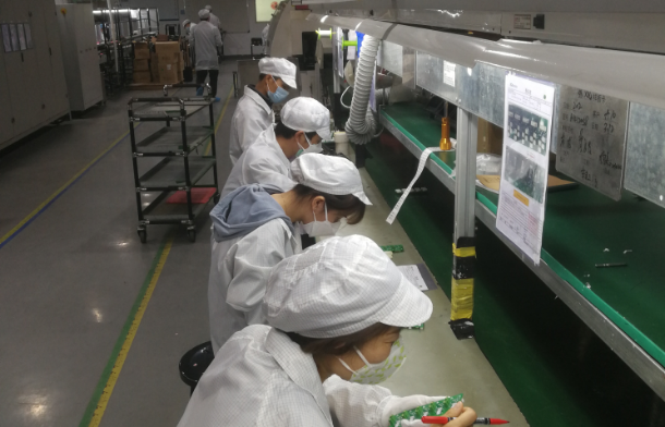
Through-hole assembly is a method for producing electronic circuits in which the components are installed through leads. It refers to the mounting process that inserts the leads to the drilled holes and solders the components on the board by wave soldering or manual soldering. In through-hole PCB assembly, the holes in the PCB are drilled or punched to precise dimensions, and the leads of the components are inserted through the holes and soldered to the PCB to create a secure electrical connection. This can be done manually or with the aid of automated equipment.
We can provide to...
- Turn times as short as 24 hours
- 1 to 100,000 units
- Class II Inspection standard and Class III Inspection available
- 100% on-time guarantee
- DFM support
- Lead free (RoHS) options
- SMT and thru-hole capabilities
- All SMT machine placed
- AOI (Automated Optical Inspection)
- Lead-free RoHS Certification and ITAR compliance screen available
-
Program Design
-
Assembly Capacity
-
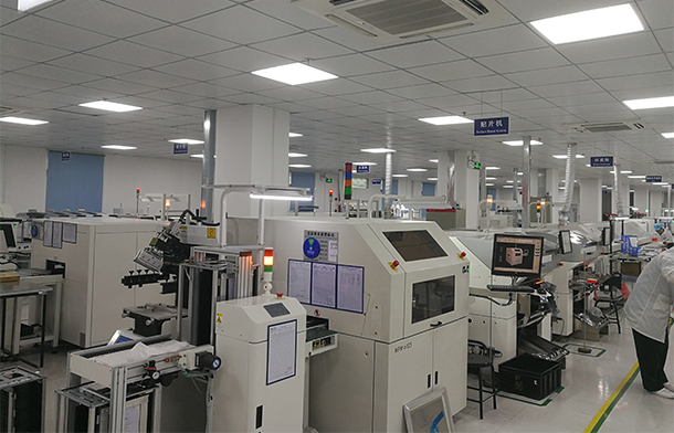
SMT Capacity
-
Equipment Exhibition
From component purchasing to function test and package finish , we provide one shop stop services for every types of PCB.
Quick payment
Flexible payment options
On-Demand Manufacturing
No MOQ or MPQ limited. Prototype or mass production order acceptable.
Inspection Of Quality
90% of the technical staff have more than 10 years of industry experience
Assembly Capacity
| Turn-key | Purchase from authorized suppliers, distributors |
| Consigned | Accept parts in reels, cut tapes, tubes & pallets and bulk. |
| Stencils | Offer Laser-cut stainless steel stencil. |
| Solder type | Offer both lead&lead-freeassembly services. |
| Board type | Rigid board, flex board&rigid-flex board. |
| PCB or Panel Size | Min board size of 10*10mm |
| PCB or Panel Size | Max board size of 330*530. |
| Assemble type | The customer provides some components |
| Board shape | There is no limit to shape |
| Prototype | MOQ as low to 5units in 1-2 days delivery |
| Low volume | Offer 3-4 days quick turn time service for low volume. |
| High volumn | Offer accurate delivery to catch your deadline. |
SMT Capacity
| Single and double sided SMT/PTH | Yes |
| Large parts on both sides | Yes |
| BGA on both sides | Yes |
| Smallest Chips size | 201 |
| Min BGA | 0.008 in. (0.2mm) pitch |
| Micro BGA pitch | ball count greater than 1000 |
| Min Leaded parts pitch | 0.008 in. (0.2 mm) |
| Max Parts size | 2.2 in. x 2.2 in. x 0.6 in. |
| Odd form parts: | Yes,Assembly by hands |
| LED | Yes,Assembly by hands |
| Wave soldering | Yes |
| Max PCB size | 14.5 in. x 19.5 in. |
| Min PCB Thickness | 0.02 |
| Fiducial Marks | Preferred but not required |
| PCB Finish: | SMOBC/HASL |
| PCB Finish: | Electrolytic gold |
| PCB Finish: | Electroless gold |
| PCB Finish: | Electroless silver |
| Ball counts | ball count greater than 1000 |
| Resistor | Yes,Assembly by hands |
| Capacitor networks | Yes,Assembly by hands |
| Electrolytic capacitors | Yes,Assembly by hands |
| Variable resistors、capacitors (pots) | Yes,Assembly by hands |
| Sockets | Yes,Assembly by hands |
| PCB Shape | Any |
| Panelized PCB | Tab routed |
| Panelized PCB | Breakaway tabs |
| Panelized PCB | V-Scored |
| Panelized PCB | Routed+ V scored |
| Inspection | X-ray analysis |
| Inspection | Microscope to 20X |
| Rework | BGA removal and replacement station |
| PCB Finish: | Immersion gold |
| PCB Finish: | Immersion tin |
| PCB Finish: | OSP |
Testing Procedures
There are several advantages to through-hole PCB assembly, including:
- High reliability: The components are securely anchored to the PCB, making the assembly less prone to failure due to mechanical stress or vibration.
- Ease of repair: If a component fails, it is relatively easy to remove and replace it using through-hole PCB assembly.
- High current capacity: The larger hole size and longer lead length in through-hole PCB assembly allows for higher current capacity compared to surface mount components.
However, through-hole PCB assembly has some disadvantages compared to surface mount technology, including:
- Higher cost: Through-hole PCB assembly is generally more labor-intensive and requires more expensive equipment, making it more expensive than surface mount assembly.
- Larger size: The components and PCBs used in through-hole assembly are typically larger than surface mount components, which can be an issue for compact designs.
- Lower density: Through-hole PCB assembly is generally less dense than surface mount assembly, which can be an issue for high-density designs.
Despite these disadvantages, through-hole PCB assembly is still used in a variety of applications where the advantages outweigh the costs, including military, aerospace, and medical equipment.


Bring you better PCB products
Circuit Board Fabrication and PCB Assembly Turnkey Services
Frequently asked questions
What is through-hole PCB assembly?
What are the advantages of through-hole PCB assembly?
What are the disadvantages of through-hole PCB assembly?
What are the steps in through-hole PCB assembly?
What tools and equipment are used in through-hole PCB assembly?
How can I ensure the quality of my through-hole PCB assembly?
The received assembled PCB's worked flawlessly. The placement of the parts is excellent. I had a very good contact with Mis wang the WINOW engineer who took care of our project. She asked the right questions to make sure the project was finished correctly. We had a very pleasant communication, fast and to the point.
This board is needed to charge the lipo batteries of my robotic platform (rover). First time order with excellent communications throughout the ordering, manufacturing progress and up to delivery tracking. Very good price especially the first order with a discount credit.
Boards arrived yesterday and got started on assembly. Excellent, solder wetting, clean line
definition, via drill holes exactly in the middle of via lands.
Please pass my thanks back to one and all who made such excellent boards.
Why Choose Us?
Since 2018, WINOW has offered good-quality PCBs with excellent turnaround times and customer satisfaction. We are one of the biggest and most skilled board manufacturers in China.
-
 Prototype orders placed within 24 hours
-
Normal lead time (5-7 Working days for some PCBs prototypes and small batch production)
-
Faster lead time (48 hours for some PCBs prototypes and small batch production)
Quick payment
Flexible payment options
On-Demand Manufacturing
No MOQ or MPQ limited. Prototype or mass production order acceptable.
Inspection Of Quality
90% of the technical staff have more than 10 years of industry experience
Technical Strength
ICT test, veneer test, aging test, ATE test can be adjusted at any time PCB Assembly according to customer requirements